Drop Test
- Test summary/features
-
Developments such as the rise of mobile electronic devices, growth of connections accompanying more advanced functions, and decrease in junction strength caused by finer junctions are resulting in more demanding environments for electronic devices in terms of reliability and quality assurance.
Mobile phones, laptops and other mobile devices are particularly prone to shocks from being dropped during use, creating the need to evaluate their environmental resistance beforehand by subjecting them to drops.
- Test equipment
-
Tests are done in compliance with standards such as JEDEC (JEDEC JESD22-B111), which specify drop test methods for PCBs.
The samples subjected to these tests are surface-mount components commonly used in mobile equipment, such as BGA, LGA, CSP, TSOP and QFN devices. The test devices are mounted in daisy chain circuitry on test boards for evaluation.
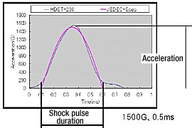
Test samples are dropped 30 times or until reaching an 80% failure rate. A 1,500 G, 0.5 ms, half-sine shock pulse is generated as the drop condition. A detected instantaneous interruption of at least 1 µ sec is regarded as a failure.
- Equipment particulars
-
- Drop Test System (installed at Utsunomiya Test Center)
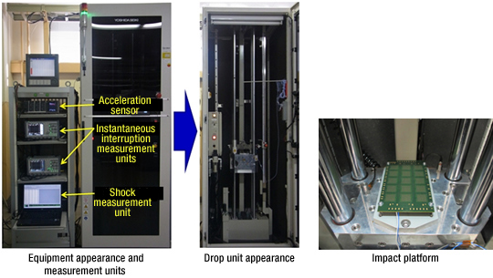
| Main specifications | |
| Impact platform dimensions | 150×160mm |
| Maximum specimen weight | 1kg |
| Maximum drop height | 1500mm |
| Shock pulse waveform | Half-sine wave |
| Impact acceleration | 550 to 2,000 G; 0.5 ± 0.05 ms duration |
| 400 to 1500G; 1.0 ± 0.1ms | |
| Automatic repeat function | Up to 9,999 times |
| Instantaneous interruption measurement | 1 µsec; up to 4 channels |
| Strain measurement | Up to 12 channels |
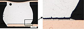
Drop impact failure example
-
Example of cross-section observation of evaluated PCB that failed
Cracking has occurred in intermetallic compound between solder ball and copper pattern, causing junction failure.Reported methods for improving drop impact resistance include:
- Applying underfill
- Reducing weight of mounted boards and semiconductor packages
- Changing solder pad plating material