>> P.2
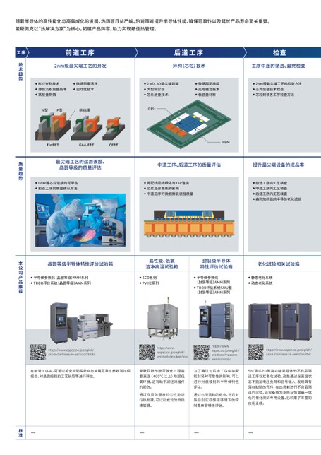
Front-endprocessBack-endprocessDevelopmentofleading-edgeprocessesof2nmlevel.Chipletandheterogeneoustechnology◆EUVLithography◆Thinfilmdeposition,layeringtechnology◆Highaspectratioetching◆Nano-scalecleaning◆Automatedtechnology◆Advanced2.xD3Dpackage◆Interposer◆Chipstackingtechnology◆Fineredistributionlayer(RDL)◆Optoelectronicintegrationtechnology◆Low-KmaterialsN-typeP-typeInsulatingfilmGPUInspectionThescreeningprocessandfinalinspection◆Inspectionforadvancedthe2nmprocess◆Chipletimplementationinspectionprocess◆InspectionmethodsforeachchipletimplementingprocessFinFETGAA-FETCFETHBMIssuesofadvancedprocessoperations,qualityevaluationatthewaferlevelQualityofthefineimplementationprocessintmiddle-endprocessYieldimprovementofadvanceddevices◆ReliabilityofchipbondingsuchasCoW◆FinerredistributionlayersandTSVconnection◆Processinspectioninthefront-end◆Methodstocheckqualityinthefront-endprocess◆Affectoflocalheatgenerationofchips◆Qualityofthefineimplementationprocessintmiddle-endprocessprocess◆Processinspectioninthemiddle-endprocess◆Processinspectionintheback-endprocess◆Burn-intestforAdvancedSemiconductorWaferlevelsemiconductorcharacteristicsevaluationequipmentHigh-performance,PackagelevelsemiconductorAnaerobicCleanOvencharacteristicsevaluationequipmentBurn-intestproducts◆SemiconductorParametric(WaferLevel)AMMSeries◆TDDBEvaluationSystem(WaferLevel)AMMSeries◆SCOSeries◆PVHCSeries◆SemiconductorParametrictestsystem(PackageLevel)AMMSeries◆TDDBEvaluationSystemSMUType(PackageLevel)AMMSeries◆StaticBurn-InSystem◆DynamicBurn-InSystemProcessTechnologytrendQualitytrendOurproposalproductsThehigh-speedprocessingandadvancedfunctionalityofsemiconductorssignificantlyimpactthermaldesignchallenges.“Thermalmanagementinsemiconductorsisessentialforperformanceenhancement,reliabilityassurance,andproductlongevity.”ESPECproposesandsupportsoptimalevaluationmethodsforsemiconductorassessmentinthermalmanagement.https://www.espec.co.jp/english/products/measure-semicon/tddb/Thisequipmentevaluatesprocessdefectsinthewaferprocessusingparametertestingincombinationwithafull-autoprober.https://www.espec.co.jp/english/products/env-test/sco/https://www.espec.co.jp/english/products/measure-semicon/spa/https://www.espec.co.jp/english/products/measure-semicon/rbs/Mitigatethedevicesinhightemperatureenvironmentrequiredforpolyimidetoimidize(400°Cormore)byprovidinganultra-lowoxygenatmosphere.Uniforminsulatinglayerfilmcanbeformedbyheattreatmentwithhightemperaturedistributionperformance.Thisequipmenttestssemiconductorparameterstoverifyprocessissuesafterpackaging.Withatemperaturechamber,transistorcharacteristicscanbeevaluatedatthepackagelevelinrealtimeunderaconstanttemperatureenvironment.Aspartofburn-intests,thereisaprocesstoscreendefectiveadvanceddevicessuchasSoCsandGPUs.Productsbeingtestedaresubjectedtovoltageloadorinputsignalsathightemperaturestofindandselectpotentiallydefectivedevicesbeforeshipping.Thisequipmentintegratestheaboveasanall-in-onetestingsystemwithatemperaturechamberandhasbeendeliveredtomanycustomers.————————StandardCE
 | <
| <  |
|  > |
> |  >>
>>